
TSMC is strengthening its position in the silicon photonics space, aiming to replicate its advanced packaging success with the COUPE (Compact Universal Photonic Engine) platform. COUPE integrates electronic ICs, photonic circuits, and advanced packaging in a system-level approach that competitors find hard to match, targeting next-generation co-packaged optics (CPO) for AI and high-performance computing.
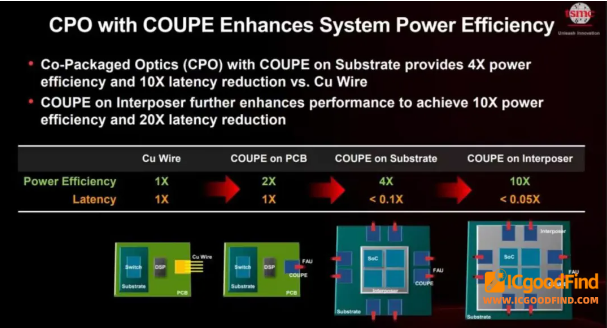
According to TSMC, COUPE can cut power consumption by 40% at the same data rate or increase speed by 170% at the same power, compared to conventional micro-bump packaging. Bit-level energy efficiency is also improving: from >30pJ per bit for traditional copper, to below 5pJ for substrate-based CPO, and potentially under 2pJ when optical I/O moves to the interposer.
TSMC's COUPE builds on its SoIC advanced packaging technology. It uses copper‑copper and hybrid bonding to directly connect electronic ICs (EIC) with wafer‑level photonic ICs (PIC). The PIC integrates key components including a 200G micro‑ring modulator (MRM) . Manufacturing involves forming an oxide layer on the wafer, bonding it to another silicon wafer, and etching vias from the backside to establish electrical paths to the substrate.

At the 2025 IEEE ECTC, TSMC’s photonics team detailed a new broadband optical engine (BOE) architecture, combining three modules: COUPE, COI (complementary optical interconnect) , and iFAU (integrated fiber array unit) . The system enables CPO integration within a 2.5D CoWoS package.
COI is the core of the BOE – a low‑loss optical routing structure consisting of paired couplers and precision waveguides. It efficiently directs light from iFAU fiber inputs to on‑chip waveguides, minimizing insertion loss – a key factor for high‑performance photonic‑electronic co‑integration.
A critical advantage of BOE is its wafer‑level manufacturability. The design uses vertical optical coupling, which is more tolerant to wafer warpage and assembly variations than edge‑coupling alternatives – improving production stability and yield. TSMC tested entire 300mm wafers, correlating optical measurements with simulations to identify process sensitivities including waveguide width, etch depth, sidewall profile, and alignment accuracy. Even minor variations in these parameters can increase optical loss and degrade signal quality.
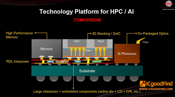
TSMC plans to expand its CPO offerings through its established CoWoS and SoIC platforms, with the BOE broadband optical engine serving as a building block for future ultra‑high‑bandwidth, energy‑efficient AI networks.
ICgoodFind Takeaway:
TSMC’s COUPE platform shows that silicon photonics is moving from lab to fab. With wafer‑scale integration and solid process control, CPO is poised to become a key enabler for next‑gen AI interconnects.
